
a, Conceptual illustration of the strain tunable single-photon source. b, Structure of the integrated FP microcavity and electric field distribution of fundamental mode. c, 3D-FDTD simulation design.

a, Monolithic FP thin-film microcavity integrated with a piezoelectric substrate under an optical microscope. b, Fluorescence imaging of the QD coupled to the microcavity. c, QD emission sweep over the microcavity mode. d, Enhancement of brightness when the QD is coupled to the cavity fundamental mode.
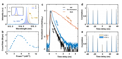
a, Coupling of the QD with the H-polarized mode. b, Rabi oscillations under resonant pulsed resonance excitation. c, Lifetime measurement. d, Single-photon purity. e, Single photon indistinguishability.
Newswise — Self-assembled semiconductor quantum dots (QDs) represent a three-dimensional confined nanostructure with discrete energy levels, which are similar to atoms. They have the capability to produce highly efficient and indistinguishable single photons on demand, holding significant importance for exploring fundamental quantum physics and various applications in quantum information technologies. Leveraging traditional semiconductor processes, this material system also offers a natural integration-compatible and scalable platform.
For an ideal QD single-photon source, a widely adopted approach to achieving photons with both high extraction efficiency and indistinguishability, is embedding QDs into Purcell-enhanced photonic cavities. However, the spatially random distribution of QDs makes it challenging to deterministically couple them with photonic structures. Currently, precise alignment of their spatial positions relies on accurate optical fluorescence positioning techniques, and one of the optimal strategies for wavelength alignment involves introducing stress tuning. The current state-of-the-art QD single-photon sources are based on open FP cavity structures or elliptical micropillars. The former achieves alignment of position and wavelength by finely tuning the top and bottom mirrors, but discrete structures are sensitive to environmental vibrations. The latter's isolated structure hinders stress transfer, making effective wavelength tuning challenging. Currently, this structure still relies on temperature tuning within a small range, significantly reducing the device yield. Achieving effective integration of stress tuning in a microcavity structure, while ensuring precise alignment of spatial position and wavelength, remains a formidable challenge.
To address these challenges, in a recent study (https://doi.org/10.1038/s41377-024-01384-7) featured in Light Science & Application, the collaborative efforts of Jiawei Yang, Ying Yu, Siyuan Yu from Sun Yat-sen University, and Yan Chen from National University of Defense Technology innovatively combined FP microcavities with piezoelectric actuator, developing a monolithic wavelength-tunable microcavity structure. This innovative approach eliminates the need for etching semiconductor materials, preventing surface defects and facilitating effective stress conduction.
As shown in Figure 1a, the designed FP microcavity in this work is integrated on a piezoelectric substrate. As QDs are located in the thin film, stress can be effectively transmitted. This structure does not require etching of semiconductor materials, effectively avoiding the influence of sidewall defects on QD emission. In the FP microcavity structure depicted in Figure 1b, the vertical confinement of the optical field is formed by upper and lower Bragg reflectors, while the lateral confinement of the optical field is created by a parabolic SiO2 defect. The simulated efficiency of the single-photon source can reach 0.95, with a Purcell factor of 40 (Figure 1c). Additionally, the fundamental mode has a Gaussian-like far-field distribution, facilitating coupling into optical fibers.
In the experimental implementation, high-precision wide-field optical positioning technology was used to place QDs at the center of the FP microcavities (Figure 2b). Subsequently, the thin-film microcavity containing a single QD was integrated onto a PMN-PT (100) substrate using micro-transfer printing technology (Figure 2a). A tuning range of 1.3 nm was achieved through voltage scanning (Figure 2c), which is the largest wavelength tuning range reported for all microcavity structures to date. A remarkable 50-fold enhancement in brightness is obtained when brought the QD with the microcavity fundamental mode, a 50-fold enhancement of brightness is achieved (Figure 2d). Furthermore, when the QD coupled with the H-polarized mode (Figure 3a), a peak APD count rate of 2.88 Mcps is recorded under pulse resonance fluorescence (Figure 3b), with an extracted polarized single-photon extraction efficiency of 0.58 and a rapid 100 ps lifetime. Compared to QDs in planar structures, this represents a tenfold reduction in lifetime (Figure 3c). The Hanbury Brown and Twiss correlation measurement extracts a single-photon purity of 0.956 (Figure 3d), signifying a low multi-photon probability. Two-photon interference experiments underscore an impressive photon indistinguishability of 0.922 (Figure 3e).
In summary, the researchers have developed a monolithic FP microcavity structure with the advantage of optimal exploitation of the Purcell effect, a compact footprint and integration capabilities. By deterministic embedding of a single QD into the microcavity, high-performance single photon sources with simultaneous high extraction efficiency, high purity, and high indistinguishability are achieved. Considering future developments, firstly, charge stabilization or spin injection using electrical gated-devices can be directly implemented in the structure to realize low-noise single-photon emission or spin-photon entanglement/ a linear cluster state. Secondly, strain tuning can also be employed to erase the spectral inhomogeneity between different QDs and addressing the FSS. These aspects are pivotal in the realization of high-performance source of entangled photon pairs. Most intriguingly, the simplicity and versatility of the cavity scheme open avenues for establishing a new manufacturing paradigm for quantum light sources, in which multiple types of solid quantum light sources (including semiconductor QDs, defects et al.) with different emitter materials and operating wavelengths could be co-manufactured on the same PMN-PT platform. This potential breakthrough could significantly advance scalable quantum photonic technologies in the future.
###
References
DOI
Original Source URL
https://doi.org/10.1038/s41377-024-01384-7
Funding information
This work is supported by Science and Technology Program of Guangzhou (202103030001), the Innovation Program for Quantum Science and Technology (2021ZD0301400, 2021ZD0301605), the National Key R&D Program of Guang-dong Province (2020B0303020001), the National Natural Science Foundation of China (12074442, 12074433, 12174447), the Natural Science Foundation of Hunan Province (2021JJ20051), the science and technology innovation Program of Hunan Province (2021RC3084), and the research program of national university of defense technology (ZK21-01, 22-ZZCX-067).
About Light: Science & Applications
The Light: Science & Applications will primarily publish new research results in cutting-edge and emerging topics in optics and photonics, as well as covering traditional topics in optical engineering. The journal will publish original articles and reviews that are of high quality, high interest and far-reaching consequence.
MEDIA CONTACT
Register for reporter access to contact detailsArticle Multimedia

Credit: Light: Science & Applications
Caption: a, Conceptual illustration of the strain tunable single-photon source. b, Structure of the integrated FP microcavity and electric field distribution of fundamental mode. c, 3D-FDTD simulation design.

Credit: Light: Science & Applications
Caption: a, Monolithic FP thin-film microcavity integrated with a piezoelectric substrate under an optical microscope. b, Fluorescence imaging of the QD coupled to the microcavity. c, QD emission sweep over the microcavity mode. d, Enhancement of brightness when the QD is coupled to the cavity fundamental mode.

Credit: Light: Science & Applications
Caption: a, Coupling of the QD with the H-polarized mode. b, Rabi oscillations under resonant pulsed resonance excitation. c, Lifetime measurement. d, Single-photon purity. e, Single photon indistinguishability.